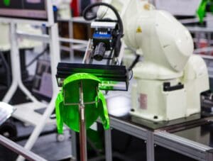
Laser metrology has substantial applications in semiconductor manufacturing for providing exact optical measurements and ensuring high quality of the products.
Laser metrology involves the application of laser beams for measuring different parts and sub-parts of the products. However, most naturally occurring laser beams are less suitable for industrial laser applications as they display a Gaussian-like intensity distribution pattern.
The Gaussian distribution pattern causes a substantial energy loss because of gradually decaying edges. Laser metrology uses different techniques, including laser beam shaping and splitting to solve this issue and modify the laser beam. For instance, a top hat beam shaper uses diffractive optical elements or DOEs to shape the beam profile and achieve a top hat distribution pattern, whereas an optical diffuser diffuses the optical energy of the beam profile by spreading the incident beam’s optical power. To do so, the optical diffuser design considers several factors, including the desired shape, wavelength, and intensity of the beam profile.
The Application of Laser Metrology in Semiconductor Manufacturing
In semiconductor manufacturing, laser metrology equipment plays a crucial role. A laser interferometer is one such piece of equipment which is useful for passively scanning and characterizing substrates. Being a non-destructive optical method, this method is a popular choice. Another reason behind the wide adoption of laser scanning metrology by the semiconductor industry is that laser metrology offers high accuracy, precision, and sensitivity. Laser metrology has critical applications in various segments of the semiconductor industry, including photolithography, critical dimension, scratch and deposition, overlay, flatness and topography, and defect inspection.
Why is Laser Metrology Important in Semiconductor Manufacturing?
Semiconductor fabrication facilities emphasize maximizing yield and throughput. This drives the incorporation of tools for wafer inspection into the production lines. These tools deliver real-time 3D data for optimizing processes, enabling precise measurements of nanometric features, wafer bow, roughness, defect detection, and film thickness. The use of high-precision machinery helps in developing high-quality devices. As a result, the quality of the consumer products improves and yield increases.
Challenges in Laser Metrology
Despite various crucial advantages of laser metrology in semiconductor manufacturing, there are certain challenges in laser metrology. While laser metrology offers accurate measurements, it requires cutting-edge components and equipment to ensure precision and diminish noise. Advanced optical solutions are required for high-resolution measurements. One such example is the measurement of small features in the semiconductor, produced by extreme ultraviolet lithography. Laser metrology scanning is a useful method for measuring these small features. Modern laser metrology uses elongated focus diffractive optical elements or DOEs to increase the range of detection and boost resolution. Diffractive optical elements of DOEs offer an ideal solution for laser metrology by providing high precision, durability, customization, and design flexibility. These optical components modify the incident laser beam to achieve a desired intensity profile.
